What Customers are Saying About Golden Gate Graphics PCB Design
- "You revolutionized our design process."
~B.H., Senior Staff Engineer - "Our board for the International Space Station has been in service since 2003 with no hardware failures. In fact, all the designs you did for me were all single-rev."
~BSZ, Senior Systems Engineer, RT Logic.
Streamlined PCB Design

PCB layout can use technologies from simple to advanced. We help you get the job done while focusing on cost-effectiveness. You can count on us to make your circuit design testable, manufacturable and accurate. The technologies we embrace include fine-pitch surface mount, transmission line routing, constraints-based placement and routing, differential impedance, analog (including RF to 6 GHz), LVDS, Memory, ECL, and LVPECL. Some of these are described below.
Controlled Impedance We use formulas for controlled impedance that are actually manufacturable and produce predictable results. Of course, you are more likely than us to have the empirical formulas you want employed. We can recommend a board house that specializes in this area by manufacturing and testing to your controlled impedance requirements. We design for testability as well as functionality.High Speed Circuitry We work closely with engineers to produce the qualities they look for in RF and ECL designs. And yes, we have worked in microwave frequencies.
High Voltage We work from UL guidelines and engineers' test results to design high voltage circuits that function properly from the first time they are switched on.
High Density Do you use fine pitch surface mount devices such as thin quad flat pack (TQFP) and ball grid array (BGA) components in multilayer designs? Whatever is needed we will design in the most cost effective manner to get your circuits into the available space. And we consult with your board and assembly houses to make sure they can work with the final design. With our know-how, we can avoid the pitfalls of blind and buried vias, the main drawback being the extreme expense of building the boards. Good, basic PCB layout methods give workable results.
Flex Circuits Flex circuits are printed circuits done in thin, flexible material. Space for conductors tend to be at a premium in flex circuits. We have plenty of experience designing them to match the advanced technology of today's specialty board houses.
Chip on Board In this technology integrated circuits are glued and wire-bonded directly to PCB's instead of first being packaged. The electronics for many mass-produced toys are embedded by this system, which can be identified by the black glob of plastic sitting on the board. Underneath that glob (technical term: gloss/pcgloG.php#"https://www.goldengategraphics.com/gloss/pcgloG.php#glob top" > glob top ), is a chip with fine wires bonded to both it and the PCB. We design chip on board to the capabilities of the wire bonding system being implemented. Because we address the controlling factors thoroughly, our chip on board layouts are manufacturable.
DUT boards
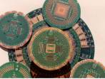
DUT stands for Device Under Test. DUT boards are used in automated
chip testing. They are part of the interface between the integrated circuit and
a test head, which in turn attaches to computerized test equipment. The
specific test equipment used will determine the value of the controlled
impedance required for the chip tester boards.

In partnership with a high-tech board house, we can implement a cost-effective DUT board system for your chip testing, whether high-volume or prototype. Email our representative and include information on which test system you will be using and which package styles you need to test.
Important Question: How did we garner all this experience?
Obviously, for each technology employed there had to be that first time, when all we knew was how to study and how to communicate. That is the most important message here, because chances are you have a technology that is pushing the edge and about which we may need to know more. You can count on us to listen and learn and (Need we say it again?) duplicate your intentions.
More than 430 Printed Circuits Designed
... and another 245 boards upgraded. (As of 1998)
While printed circuits are very similar from one application to another, there are differences based on space available, type of circuitry and even environment of end-use.
Our designers have worked with over 70 electronics companies, from independent consultants to large corporations. Here are some of the hardware applications our successful PCB layout methods have addressed:
| audio | aerospace communications |
| athletic equipment | chip based transponders |
| disk drives | DUT boards (chip testing) |
| electronics testing | fighter-jet avionics |
| geophysical instruments | (Geomation, Inc.) |
| human heart assist pump | (Biomedical Research Associates and Jarvik Heart, Inc.) |
| high speed, high voltage amplifiers | (CMED IPS - Colorado MedTech Imaging and Power Systems Div.) |
| image scanners | image processing |
| medical diagnostics | memory |
| power supplies | remote control |
| satellite-implemented, centralized monitoring of remote sites | (Nova-Net Communications, Inc. div. of Stratos, Inc.) |
| servo motor controls | |
| space exploration experiments | (LASP - CU's Laboratory of Atmospheric and Space Physics ) |
| telecommunications | |
| telescope control | DFM Engineering, Inc. with computer-controlled telescope installations worldwide, including CU's Sommers-Bausch Observatory , which is "OPEN for FREE stargazing & planet-watching on Friday nights after 8:00pm (weather permitting)!" |
| ultrasound | (Tetrad, Inc. and Fischer Imaging Corp.) |
| video & graphics | |
| wind energy experiments | (NREL - National Renewable Energy Lab) |
| X ray |
Our designers have expertise in many varieties of software :
| In the past we have used many varieties of PCB layout and schematic capture software. Your old databases might be editable, so check with us on a case-by-case basis. Here is a description of our software capability in various database formats. |


We also make our experience available to your company. If you have just acquired a CAD system, we may be able to help you implement it. We have extensive experience with personal computers and CAE/CAD applied to electronic circuitry.
We can tutor new CAD personnel and help you get your products out the door.
If you are looking for cost-effective answers to your future CAD software needs, we can help.
Continue on, and find out how we duplicate your intentions: A typical project.


