What Customers are Saying About Golden Gate Graphics PCB Design
- "You revolutionized our design process."
~B.H., Senior Staff Engineer - "Does incredible work with footprints, libraries, directives and project setup for manufacturing. Has a complete understanding of PCB layout and communicates with you when something does not look right. PCB include : LVDS , RF, High speed digital with processors."
~Lisa S, Engineering Manager.
What Is a PCB Designer Anyway?
First, what is a PCB?
A PCB is a Printed Circuit Board. The picture below is a photograph of a simple PCB after it has been manufactured at a "board house." This PCB is called a "bare board"—it does not have any electrical components mounted on it as yet. A printed circuit board in this preliminary form has a set of copper traces called "wiring." These "wires" have been applied by a process loosely analogous to printing.
Top1533-768hIq70.webp)
Here is another example of one: Have you ever looked inside your computer, a radio or a telephone? The printed circuit boards inside it are the flat, thin, usually rectangular, commonly green fiberglass slabs that have electrical components attached. Harder to see are copper traces running underneath the green covering. You would have to try different angles of light to see them. These are wires that are "printed" on the fiberglass slab. They connect the electrical components, thus forming circuits. Thus the name "printed circuit board."
If you are looking at a PCB from some consumer electronic product, here is a statement about it that is so obvious it might be overlooked: It has been mass produced. The whole purpose of PCB design is to bring an electronic circuit (as designed by an electrical engineer) into a form that is manufacturable. That is, it would be capable of being mass produced. Whether the actual number of units was 100 or 1 million, at some level, this is mass production.
The alternative for a printed circuit board is a hand-wired board. Such a construction is impractical for mass production. It is costly and unreliable. One wire pulled loose can render it non-functional. However, if it is wired correctly, it will often perform better electrically than a PCB. Therefore, part of the technology of PCB design is to create artwork that is not only manufacturable, but performs well electrically and approaches the ideal of a hand-wired board.
A company that manufactures electronic products has a cycle of production to go from concept to end user or customer. It could be thought of like this: Marketing - Sales - Product Concept - Engineering & Design - Electrical Engineering & Circuit Design - Printed Circuit Design (Designing Artwork for Manufacturing) - Printed Circuit Board Manufacturing - Printed Circuit Assembly - Packaging - Distribution.
And now, what is a PCB designer?
The PCB designer is between the circuit designer (electrical engineer) and the printed circuit manufacturer (also called "board house"). The PCB designer gets the electronic circuit ready for manufacturing, by laying out the artwork that the board house uses.
Please understand this distinction: Printed circuit design and circuit design are entirely two different things. An electrical engineer has done the circuit design in the step just before the printed circuit design. He has produced, among other things, a diagram of the functionality of the circuit. This diagram is called a "schematic."
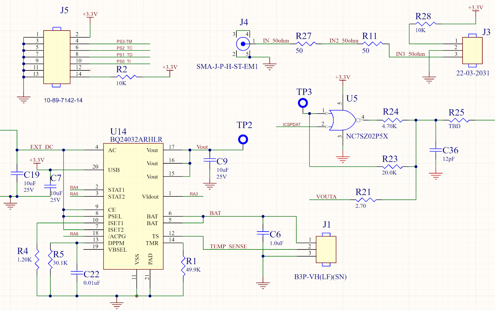
In this day and age, it would reside on a computer and be a file made by specialised software of the type Computer Aided Engineering (CAE). The example picture of a schematic is a portion of the CAE file as displayed on a computer. It contains symbols connected by lines. The green lines represent wires, electrical connections.

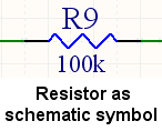
For example, a symbol with a zig-zag line is used to represent a resistor, a type of electrical component that reduces the voltage of a current that passes through it. It removes some energy and dissipates that as heat.

The little zig-zag line does not at all resemble what a resistor actually looks like. It symbolizes the function of a resistor in an intuitive way. The function represented by the zig-zag line is that it sort of "slows down" or impedes the current. A schematic diagram is composed of a variety of such symbols, not one of which looks like the real-life physical component which it represents.

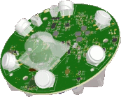
Here is a physical representation of the resistor in 3D. This picture is from our PCB design file, which has been generated and displayed by a specialized software of the type Computer Aided Design (CAD). The software we prefer at Golden Gate Graphics is Altium Designer.
So here you have an illustration of the concepts: The schematic symbol in the CAE software represents the function of the part and the PCB component in the CAD software represents its physical characteristics (size, shape, electrical terminals as metallized objects, name as text and location).
In order to manufacture a printed circuit board, it is necessary to take the design from the functional diagram or schematic and change it into a form of artwork that makes a pattern of components, holes and printed wires. This pattern is nowadays in the form of digital data and is used by a bare printed circuit board manufacturer (aka "board house") to control their photographic imaging techniques and computer-controlled drilling machinery, all resulting in the manufacture of the PCB. The PCB designer is the person who creates the artwork for that purpose. The artwork is analogous to the plates used in printing, it forms the pattern that is "printed" into the PCB. The process is only vaguely similar to printing. Technically it is quite different.
Here is an excellent video that fully covers the technology that the board house uses to manufacture a PCB, by Saturn Electronics Corporation of metro Detroit. PCB Fabrication Process Tour (Click here).
To carry the analogy to printing a bit farther, let's use the printing of a book as a metaphor for production of an electronic device. The author of the book is the circuit design engineer or "double-E" or electrical engineer. The typesetter is the "layout guy" or PCB designer.
So there you have it.
© 1999-2025 John Walt Childers, IPC-CID. All Rights Reserved. Revised 2025


